
Nvidia Reported to Book TSMC’s 1.6nm A16 for Feynman, Skipping the N2 Generation Entirely
Nvidia Reported to Book TSMC’s 1.6nm A16 for Feynman, Skipping the N2 Generation Entirely
Nvidia has reportedly booked capacity on TSMC’s A16 process — the foundry’s 1.6nm-class node — for its Feynman GPU architecture, with mass production placed in the second half of 2028. Reports indicate Nvidia will bypass the N2 family entirely, moving from its current generation straight to A16.
A caveat before the detail: Nvidia has not publicly confirmed this. The reporting is consistent across several outlets but is presented as supply-chain reporting rather than an announcement, and no wafer volumes or contract values have been disclosed.
What A16 brings
A16 is TSMC’s successor to its 2nm N2 family, combining gate-all-around transistors with backside power delivery — routing power through the underside of the wafer so the front side is freed for signal routing. TSMC puts A16 at 8–10% more density and speed than N2P, with 15–20% lower power. Production readiness for the node is given as the second half of 2026, roughly two years ahead of the Feynman parts that would use it.
The packaging is the real story
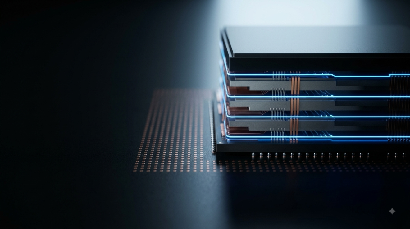
Feynman is reported to move past the planar chiplet arrangements of the current generation to vertical stacking using TSMC’s SoIC technology, alongside CoWoS-L 2.5D integration and next-generation panel-level packaging. Co-packaged optics via TSMC’s COUPE photonic engine are also reported.
Bandwidth figures quoted for Feynman are worth treating carefully. Reports cite over 1,000 TB/s of total system bandwidth against Rubin’s 520 Tb/s — but those two figures use different units as published, so they should not be read as a like-for-like multiple until Nvidia states the numbers itself.
Why an embedded audience should care about a datacentre GPU
It is fair to ask what a 2028 AI accelerator has to do with anyone building industrial sensors or gateways. Two things, and neither is about the GPU itself.
The first is capacity. When a customer of Nvidia’s scale books a leading-edge node years ahead, it moves the queue behind it. Foundry capital follows the leading edge, and the mature nodes that actually carry embedded work — the 28nm, 40nm and 65nm processes that most MCUs, PMICs and sensor front-ends are built on — compete for the same tool installs, the same substrate supply and increasingly the same advanced-packaging capacity. Lead times and pricing on parts that have nothing to do with AI have been moved by exactly this dynamic before.
The second is where the industry’s value is migrating. Feynman’s headline is a process node, but its substance is SoIC stacking, panel-level packaging and co-packaged optics. That is a packaging story. It is also, not coincidentally, precisely the layer India has chosen to enter — Micron at Sanand, Kaynes Semicon’s OSAT, CG Semi’s pilot line and Tata’s Jagiroad ATMP are all assembly, test and packaging plays, not wafer fabs. The conventional read is that India started with packaging because fabs are harder. The more interesting read is that packaging is where an increasing share of performance now comes from, and that the ATMP-first path may prove better timed than it looked when it was chosen. Advanced packaging is a different discipline from the wire-bond and flip-chip work these plants are commissioning today — but it is a ladder with rungs, and India is now standing on the bottom one.
Whether Nvidia confirms the A16 booking or not, the direction it points is the one to watch: performance is increasingly bought with stacking and interconnect rather than lithography alone.
Related articles
- SEMICON India 2026 Opens Today With 600+ Exhibitors — and One Scorecard Worth Watching18 September 2026
- Tata Electronics’ ₹27,000 Crore Jagiroad ATMP Plant Targets Production in FY2026–274 June 2026
- Tata Electronics and ASML Sign MoU to Power India’s First 300mm Semiconductor Fab in Dholera28 May 2026
- Semicon India 2025: India’s Leap Towards Becoming a Global Semiconductor Powerhouse3 September 2025
- India’s Semiconductor Surge: Building a Million Jobs in IoT & Embedded Systems by 202611 June 2025