
Tata Electronics and ASML Sign MoU to Power India’s First 300mm Semiconductor Fab in Dholera
Tata Electronics and ASML Sign MoU to Power India’s First 300mm Semiconductor Fab in Dholera
ASML’s lithography tools, talent development, and supply chain support will underpin the ₹91,000 crore fab’s ramp-up in Gujarat
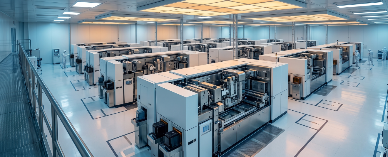
Tata Electronics and ASML have signed a Memorandum of Understanding (MoU) to advance India’s semiconductor manufacturing ecosystem, with ASML committing its lithography tools and services to support the ramp-up of Tata Electronics’ upcoming 300 mm (12-inch) fab in Dholera, Gujarat. The announcement was made on May 16, 2026.
The Dholera fab is India’s first commercial 300 mm semiconductor facility, backed by a planned total investment of US$11 billion (approximately ₹91,000 crore). It will manufacture chips for automotive, mobile, AI, and other segments, targeting global customers.
What the Partnership Covers
The MoU covers three areas: lithography deployment, talent development, and supply chain resilience.
On the equipment side, ASML will deploy its full suite of lithography systems — both DUV (Deep Ultraviolet) and related tools — to support fab operations. Lithography is the most critical and cost-intensive step in chip fabrication, used to pattern circuit features onto silicon wafers. ASML holds a near-monopoly on advanced lithography systems globally, making this partnership structurally significant for the Dholera fab’s ability to operate and scale.
On talent, the two companies will jointly develop training programmes to build a domestic pool of lithography-skilled engineers. The availability of qualified engineers locally is a known bottleneck for India’s semiconductor ambitions — most advanced fab training currently happens offshore.
The third pillar covers R&D infrastructure and supply chain resilience, with both companies working to establish long-term manufacturing and process support within India.
Fab Technology Snapshot
| Parameter | Detail |
| Wafer Size | 300 mm (12 inch) |
| Location | Dholera, Gujarat, India |
| Planned Investment | US$11 billion (~₹91,000 crore) |
| Technology Nodes | 28nm, 40nm, 55nm, 90nm, 110nm |
| Technology Partner | PSMC (Powerchip Semiconductor Manufacturing Corporation, Taiwan) |
| Target Markets | Automotive, mobile, AI, industrial |
| ASML Role | Holistic lithography tools, training, supply chain, R&D support |
Quotes
Dr. Randhir Thakur, CEO & MD of Tata Electronics, stated that ASML’s expertise in holistic lithography would ensure a timely fab ramp, support supply chain resilience, and help build local semiconductor talent — describing it as a “foundational partnership” aimed at manufacturing excellence.
Christophe Fouquet, President & CEO of ASML, noted India’s expanding semiconductor sector as representing significant opportunity, and called the MoU an important milestone in establishing long-term partnerships in the region.
Why This Matters
The Tata Electronics-ASML partnership is one of the clearest signals yet that India’s semiconductor programme is moving from policy to physical infrastructure. The Dholera fab, when operational, will be the country’s first high-volume 300 mm foundry — the same wafer standard used by TSMC, Samsung, and other global fabs.
ASML’s involvement matters beyond equipment supply. The company’s willingness to commit to talent development and R&D collaboration in India signals confidence in the long-term viability of the Dholera facility. For India’s broader semiconductor ecosystem — including fabless design firms, EDA vendors, and materials suppliers — a credible, ASML-supported fab represents an anchor investment.
The announcement also aligns with the strategic technology partnership framework between India and the Netherlands, positioning this MoU within a broader diplomatic and industrial context.
What to Watch
Tata Electronics states that construction of the Dholera plant is progressing rapidly. The next milestones to track are: fab construction completion timeline, ASML equipment order specifics (DUV scanner models and quantities), and the rollout of the joint talent development programme. The partnership with ASML follows Tata Electronics’ earlier technology deal with PSMC for process know-how across the 28–110nm node range.
Related articles
- SEMICON India 2026 Opens Today With 600+ Exhibitors — and One Scorecard Worth Watching18 September 2026
- Tata Electronics’ ₹27,000 Crore Jagiroad ATMP Plant Targets Production in FY2026–274 June 2026
- Semicon India 2025: India’s Leap Towards Becoming a Global Semiconductor Powerhouse3 September 2025
- India’s Semiconductor Surge: Building a Million Jobs in IoT & Embedded Systems by 202611 June 2025
- India’s Chip Boom: $21B Investments, 40,000 Jobs, and a New Era for Electronics3 June 2025